Logic Diagrams, Transistor Level
The 2-1 multiplexer (2mux.mag)
This transistor level diagram is the simply two transmission gates
stuck put together. Using a control signal A0 and its inverse, this system
is capable of choosing between two input lines. By itself, it is not a
very good implementation, since there is a possibility of backwards
transmission, but we attach a latch immediately afterwords, to protect the
output.

The 4-1 multiplexer
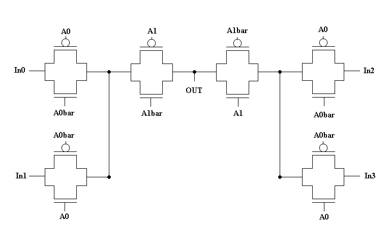
Similar to the 2-1 multiplexer, except that it can handle 4 inputs. It
has two different control lines, A0 and A1, and their associated inverses.
A latch can be added to the end to prevent backwards transmission.

The Generic Latch
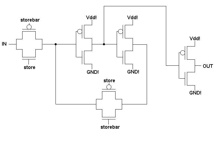
All of our latches are based on this design. We opted to go with an
output inverter, in order to protect the latch from corruption from an
output bus. Though this design requires a few more transistors, we weren't
pressed for space.

The Adder
The large transistor diagram below can add two one-bit numbers
together, considering the Carry_in as well. It outputs a sum and a carry
out. In order to accomodate 8-bit numbers, 8 of these adders are connected
together to make a ripple carry adder. The subtraction mechanism is not
included in the adder. Instead, if a number is to be subtracted, the
original number is first inverted. This inverted value is chosen through
the multiplexer, and is an input into the adder. A carry_in of 1 is also
included, since you must add 1 to an inverted number in order to actually
negate it.


